- 您现在的位置:买卖IC网 > Sheet目录305 > 93LC56AX/SN (Microchip Technology)IC EEPROM 2KBIT 3MHZ 8SOIC
�� �
�
�93AA56A/B/C,� 93LC56A/B/C,� 93C56A/B/C�
�2.0�
�FUNCTIONAL� DESCRIPTION�
�2.3�
�Data� Protection�
�When� the� ORG� pin� (93XX56C)� pin� is� connected� to�
�V� CC� ,� the� (x16)� organization� is� selected.� When� it� is�
�connected� to� ground,� the� (x8)� organization� is� selected.�
�Instructions,� addresses� and� write� data� are� clocked� into�
�the� DI� pin� on� the� rising� edge� of� the� clock� (CLK).� The� DO�
�pin� is� normally� held� in� a� High-Z� state� except� when� read-�
�ing� data� from� the� device,� or� when� checking� the� Ready/�
�Busy� status� during� a� programming� operation.� The�
�Ready/� Busy� status� can� be� verified� during� an� Erase/�
�Write� operation� by� polling� the� DO� pin;� DO� low� indicates�
�that� programming� is� still� in� progress,� while� DO� high�
�indicates� the� device� is� ready.� DO� will� enter� the� High-Z�
�state� on� the� falling� edge� of� CS.�
�All� modes� of� operation� are� inhibited� when� V� CC� is� below�
�a� typical� voltage� of� 1.5V� for� ‘93AA’� and� ‘93LC’� devices�
�or� 3.8V� for� ‘93C’� devices.�
�The� EWEN� and� EWDS� commands� give� additional�
�protection� against� accidentally� programming� during�
�normal� operation.�
�Note:� For� added� protection,� an� EWDS� command�
�should� be� performed� after� every� write�
�operation� and� an� external� 10� k� ??� pull-down�
�protection� resistor� should� be� added� to� the�
�CS� pin.�
�After� power-up,� the� device� is� automatically� in� the�
�2.1�
�Start� Condition�
�EWDS� mode.� Therefore,� an� EWEN� instruction� must� be�
�performed� before� the� initial� ERASE� or� WRITE� instruction�
�The� Start� bit� is� detected� by� the� device� if� CS� and� DI� are�
�both� high� with� respect� to� the� positive� edge� of� CLK� for�
�the� first� time.�
�can� be� executed.�
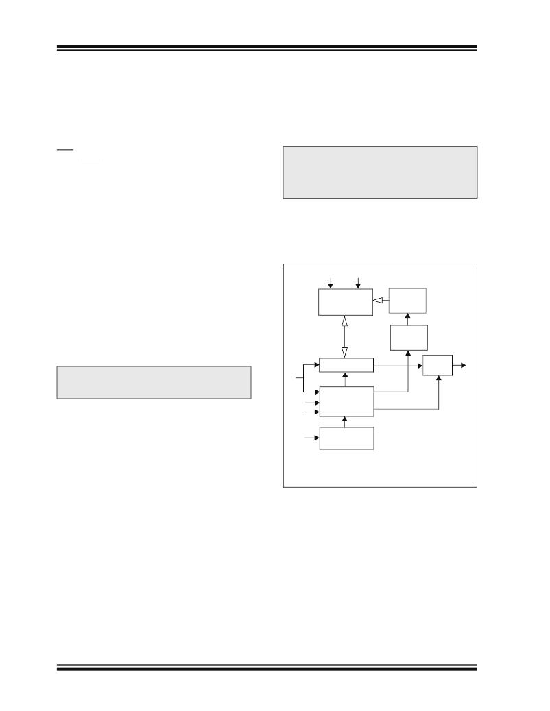
�Block� Diagram�
�Before� a� Start� condition� is� detected,� CS,� CLK� and� DI�
�may� change� in� any� combination� (except� to� that� of� a�
�V� CC�
�V� SS�
�Start� condition),� without� resulting� in� any� device�
�operation� (Read,� Write,� Erase,� EWEN,� EWDS,� ERAL�
�or� WRAL).� As� soon� as� CS� is� high,� the� device� is� no�
�longer� in� Standby� mode.�
�An� instruction� following� a� Start� condition� will� only� be�
�executed� if� the� required� opcode,� address� and� data� bits�
�Memory�
�Array�
�Address�
�Decoder�
�Address�
�Counter�
�for� any� particular� instruction� are� clocked� in.�
�Note:� When� preparing� to� transmit� an� instruction,�
�either� the� CLK� or� DI� signal� levels� must� be�
�at� a� logic� low� as� CS� is� toggled� active� high.�
�2.2�
�Data� In/Data� Out� (DI/DO)�
�It� is� possible� to� connect� the� Data� In� and� Data� Out� pins�
�together.� However,� with� this� configuration� it� is� possible�
�for� a� “bus� conflict”� to� occur� during� the� “dummy� zero”�
�DI�
�ORG*�
�CS�
�CLK�
�Data� Register�
�Mode�
�Decode�
�Logic�
�Clock�
�Register�
�Output�
�Buffer�
�DO�
�that� precedes� the� read� operation� if� A0� is� a� logic� high�
�level.� Under� such� a� condition� the� voltage� level� seen� at�
�Data� Out� is� undefined� and� will� depend� upon� the� relative�
�impedances� of� Data� Out� and� the� signal� source� driving�
�A0.� The� higher� the� current� sourcing� capability� of� A0,�
�the� higher� the� voltage� at� the� Data� Out� pin.� In� order� to�
�limit� this� current,� a� resistor� should� be� connected�
�between� DI� and� DO.�
�DS21794G-page� 6�
�*ORG� input� is� not� available� on� A/B� devices�
�?� 2003-2011� Microchip� Technology� Inc.�
�发布紧急采购,3分钟左右您将得到回复。
相关PDF资料
93LC66BXT/SN
IC EEPROM 4KBIT 2MHZ 8SOIC
93LC66XT/SN
IC EEPROM 4KBIT 2MHZ 8SOIC
93LC86/P
IC EEPROM 16KBIT 3MHZ 8DIP
94104-044LF
94104-044LF PCB MJ LOW PROFILE
94152-088LF
CONN MOD JACK 8-8 VERT PCB SHLD
9436-7600
CONN SOCKET 36POS CLOSED END
94729-002LF
6POS SNAP-IN SP.MODJACK LF
94908-588LF
588LF C/P PCB M/J
相关代理商/技术参数
93LC56AX-E/MC
制造商:MICROCHIP 制造商全称:Microchip Technology 功能描述:2K Microwire Compatible Serial EEPROM
93LC56AXE/MS
制造商:MICROCHIP 制造商全称:Microchip Technology 功能描述:2K Microwire Compatible Serial EEPROM
93LC56AX-E/MS
制造商:MICROCHIP 制造商全称:Microchip Technology 功能描述:2K Microwire Compatible Serial EEPROM
93LC56AXE/MSG
制造商:MICROCHIP 制造商全称:Microchip Technology 功能描述:2K Microwire Compatible Serial EEPROM
93LC56AXE/OT
制造商:MICROCHIP 制造商全称:Microchip Technology 功能描述:2K Microwire Compatible Serial EEPROM
93LC56AX-E/OT
制造商:MICROCHIP 制造商全称:Microchip Technology 功能描述:2K Microwire Compatible Serial EEPROM
93LC56AXE/OTG
制造商:MICROCHIP 制造商全称:Microchip Technology 功能描述:2K Microwire Compatible Serial EEPROM
93LC56AXE/P
制造商:MICROCHIP 制造商全称:Microchip Technology 功能描述:2K Microwire Compatible Serial EEPROM